As an important electrical device, field-effect transistors (FETs) play critical roles in modern electronic applications and a variety of state-of-the-art technologies including flat panel displays, memory devices, sensors, nanofluidic transistors etc. Recent research demonstrated FETs with porous channel can greatly extend their applications on voltage-gated ion channels/microfluidic chips and vastly enhance the sensitivity of FET-based gas/ ion sensors.
Conductive MOFs possessing pores of regular size-distribution, tunable structure and good electrical properties, are extremely desired to act as a promising material for porous-FET. However, up to now, MOF-based FETs have never been reported, owing in largely to the challenge in preparing high-quality conductive MOF thin films.
Prof. XU Gang’ Group from Fujian Institute of Research on the Structure of Matter, Chinese Academy of Sciences, with the cooperation of Prof. HE Jun from Guangdong University of Technology, made a significant progress on the research of self-assembled high-quality conductive MOF thin films and their applications on porous MOF-FETs.
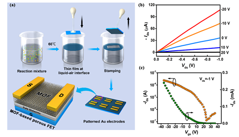
The research group prepared a high-quality conductive MOF thin film, Ni3(HITP)2 (HITP=2,3,6,7,10,11-hexaiminotriphenylenesemiquinonate), by a liquid-gas interfacial self-assembly method. Characterizations of this Ni3(HITP)2 thin film demonstrate it is ultra-flat, compact and uniform in a large scale without any steps or cracks (average surface roughness is only ~1 nm).
Then, followed by the previous development of “Modular Assembly” method (J. Am. Chem. Soc. 2012, 134, 16524; J. Am. Chem. Soc. 2013, 135, 7438), the Ni3(HITP)2 thin film can be easily transferred on a SiO2/Si wafer substrate by a simple stamping process. After depositing patterned Au electrodes, the porous FETs based a conductive MOF thin film is firstly shown.
The electrical performances of as-fabricated porous MOF-FET device demonstrate the subthreshold swing (SS) value of this device is 2.4 V/decade and the calculated interface defect density (Nt) is ~8.2´1012 cm-2, which indicates a relatively low defect density at the interface between Ni3(HITP)2 channel layer and SiO2 gate dielectric. Notably, the calculated field-effect hole mobility is as high as ~48.6 cm2 V-1 s-1 , which is comparable to the highest value reported for solution-processed organic or inorganic FETs.
Theoretical calculation indicates such high mobility may be ascribed to both of the so-called “through-bond” (within 2D layer) and “through-space” channels (among layers) for charge transport that may synergistically enhance the charge mobility in the Ni3(HITP)2 thin film. These results have been published in the form of communication in Journal of the American Chemical Society.
The results in this paper provide a step forward for both conductive MOF thin film and MOF-based devices. Moreover, the merits of MOFs like variable and designable structure, regular pore and large surface area, tunable band structure by chemical modification give us infinite imagination of its application on electronic devices in future.