Electron transfer (ET) type chromic materials can transfer electron after external stimuli, and then generate stable charge separation state. The change of electron density can modulate the electrical properties of semiconductors.
In a study published in J. Am. Chem. Soc., a research team led by Prof. GUO Guocong at Fujian Institute of Research on the Structure of Matter (FJIRSM) of the Chinese Academy of Sciences (CAS), reported an inorganic-organic hybrid nanoribbon array structure where 1-D semiconducting inorganic nanoribbons covalently bond to 1-D semiconducting organic π-aggregates.
After photo-induced ET, it yields a long-lived charge-separated state with a broad absorption band covering the 200-900 nm region.
After coloration, the conductance increased 1800 times and this contrast value represents a record for photoswitchable semiconductors.
The photoconductance also increased after coloration, and it is the first example of modifying photoconductance of semiconductors through photo-induced ET.
This work offered a new design strategy to improve absorption range, conductance, photoconductance, and stability of lead-halide semiconductors, which may help in the exploration of more light absorbers for solar cells.
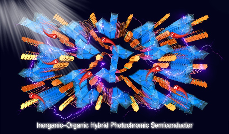
Schematic representation of chromic inorganic?organic hybrid nanoribbon array. (Image by Prof. GUO et al.)
Contact:
Prof. GUO Guocong
Fujian Institute of Research on the Structure of Matter
Chinese Academy of Sciences
Email: gcguo@fjirsm.ac.cn